Power from Potential: A Survey of Electrostatic Actuators for Haptics
arxiv.org
July 22, 2026, 1:03 p.m.
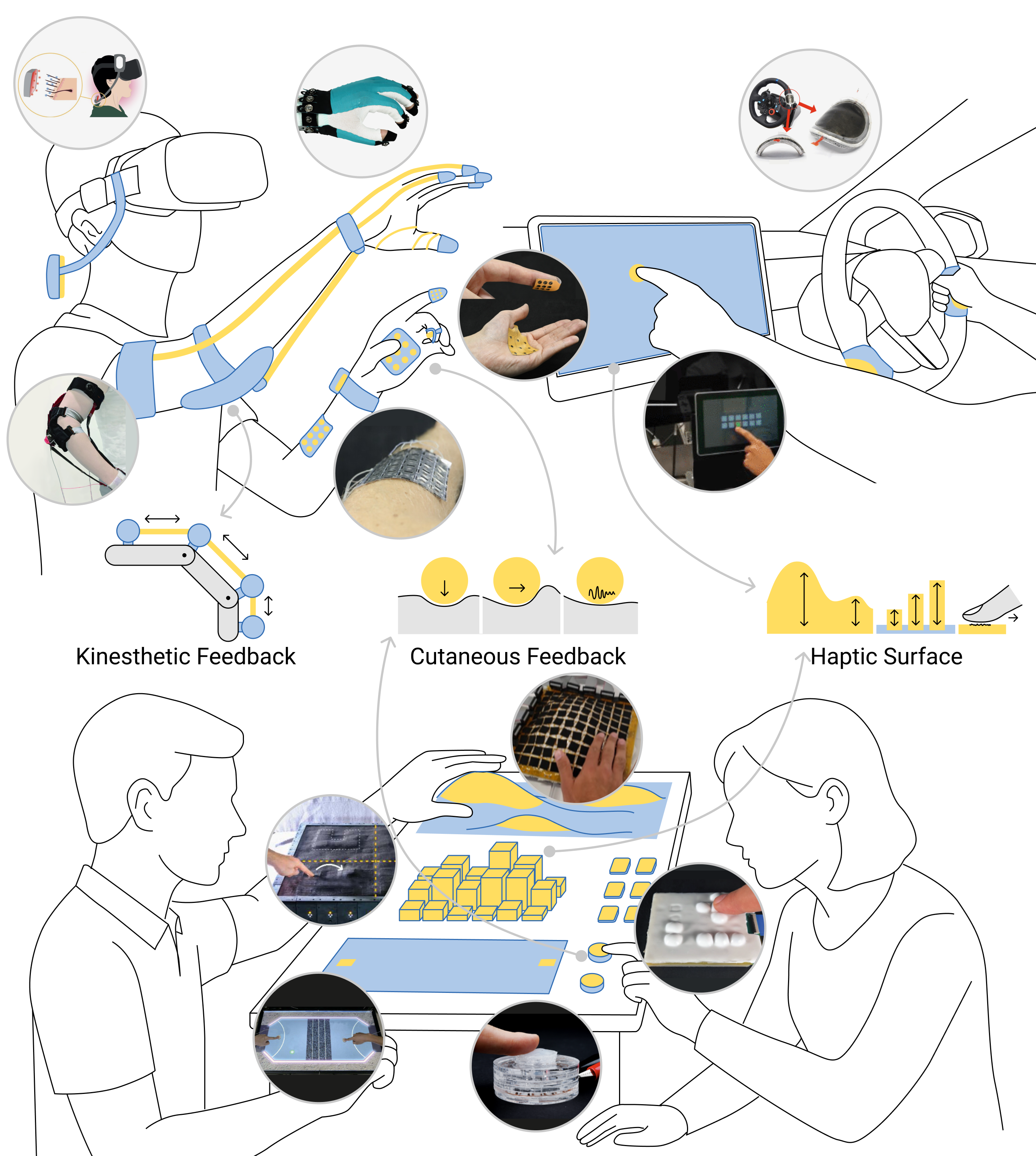
High-Voltage Electrostatic Actuators (HVEAs) represent a promising advancement for haptic interfaces integrated into wearables and everyday environments, addressing limitations of conventional actuators like DC motors and shape memory alloys. HVEAs generate force by applying electric fields to localized charge concentrations using high voltages and ultra-low currents, delivering fast, silent, and energy-efficient operation within customizable, compliant form factors. This survey examines four major HVEA classes: electrostatic switchable adhesives, dielectric elastomer actuators, soft electrohydraulic actuators, and electrokinetic pumps. The analysis characterizes each technology's bandwidth, force density, and spatial scalability for rendering both cutaneous and kinesthetic feedback across wearable and world-grounded interfaces. The research identifies common design constraints and emerging strategies for improving ergonomics, fabrication, and self-sensing integration. HVEAs are uniquely positioned to advance haptic interaction through their compact, lightweight design and fast response times, making them ideal for on-skin and seamlessly integrated applications, with key research directions needed for practical system implementation.