
Les partenariats entre la recherche publique et les entreprises | Cour des comptes
www.ccomptes.fr
July 27, 2026, 9:47 p.m.
Entre 2014 et 2024, l’État a mobilisé près de 19 Md€ de financements directs en faveur de la recherche partenariale, soit 1,7 Md€ par an en moyenne, avec un point haut de 3 Md€ en 2024. L’évaluation par la Cour de ce soutien public a mis en évidence, à l’échelle des entreprises, une corrélation entre le recours à ces partenariats, le niveau des dépenses de R&D et, dans certains cas, l’emploi. Il en ressort toutefois également que leur effet sur l’effort global de recherche des entreprises n’est pas perceptible à ce stade. La Cour constate par ailleurs que les dispositifs de soutien, nombreux et complexes, ne s’inscrivent pas dans une stratégie cohérente et restent insuffisamment évalués. Elle recommande de mieux diriger les financements vers un nombre limité de priorités nationales, d’améliorer la coordination et la qualité du service rendu aux chercheurs et aux entreprises et d’adapter les règles de gestion des carrières, des rémunérations et des activités de conseil des chercheurs afin de favoriser davantage leur engagement auprès du monde économique.
Share on

How to move biomanufacturing from lab to market
www.weforum.org
July 25, 2026, 4:03 a.m.
The global bioeconomy, valued between $4 trillion and $5 trillion, faces a critical inflection point despite biological innovations potentially reshaping 60% of physical material production. Currently, bio-based materials represent only 1-2% of global output, with even the most mature option, polylactic acid, comprising less than 1% of plastic production. Three persistent barriers—high costs, performance limitations, and absent closed-loop ecosystems—have impeded commercialization for decades. The core challenge extends beyond technical obstacles to systemic coordination failures throughout the value chain. Recognizing China's unique position as an industrial-scale testbed, supported by its 14th Five-Year Plan for Bioeconomic Development and an integrated industrial ecosystem, China Merchants Group and Cathay Biotech have developed a technology-industry-finance synergy framework. This approach combines industrial scale with synthetic biology expertise to address critical bottlenecks in feedstock supply, production efficiency, and market adoption. Early applications, including bio-based polyamide formwork for real estate projects, demonstrate how this coordinated ecosystem model can successfully transition laboratory innovations to commercial markets at scale.
Share on
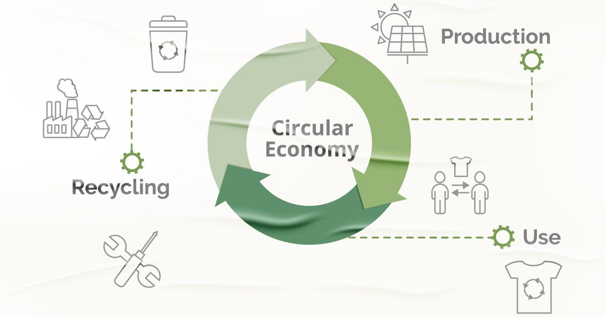
Circular Economy - Environment - European Commission
environment.ec.europa.eu
July 25, 2026, 4:02 a.m.
The European Commission is addressing global resource consumption patterns, which are projected to require three Earths' worth of materials by 2050 under the current linear economy model. The EU is transitioning to a circular economy that keeps products and materials in circulation while minimizing waste, essential for achieving climate neutrality by 2050 and building a competitive Europe. The Circular Economy Act, due for adoption in 2026, will establish a Single Market for secondary raw materials, increase recycled material supply, and stimulate demand within the EU, supporting the goal of making Europe the world leader in circular economy by 2030. Europe's circularity rate currently stands at approximately 12%, with an ambitious target to double it to 24% by 2030 as part of the EU's Clean Industrial Deal. In August 2025, the Commission launched public consultation on the upcoming act and conducted a Youth Check to assess impacts on young people, including dedicated sessions at the European Circular Economy Stakeholder Platform conference in April 2026. This legislation builds on the second Circular Economy Action Plan from March 2020, a cornerstone of the European Green Deal, addressing product design and lifecycle management to establish a resource-efficient, low-waste economy.
Share on

Material-Independent Surface Chemistry beyond Polydopamine Coating
pubs.acs.org
July 23, 2026, 6:22 p.m.
Various methods have been developed in surface chemistry to control interface properties of a solid material. A selection rule among surface chemistries is compatibility between a surface functionalization tool and a target material. For example, alkanethiol deposition on noble metal surfaces, widely known as the formation of a self-assembled monolayer (SAM), cannot be performed on oxide material surfaces. One must choose organosilane molecules to functionalize oxide surfaces. Thus, the surface chemistry strictly depends on the properties of the surface. Polydopamine coating is now generally accepted as the first toolbox for functionalization of virtually any material surface. Layer-by-layer (LbL) assembly is a widely used method to modify properties of versatile surfaces, including organic materials, metal oxides, and noble metals, along with polydopamine coating.
Share on

France 2030 : un bilan à mi-parcours prometteur, des leviers pour amplifier l’impact
www.info.gouv.fr
July 22, 2026, 6:53 p.m.
Les évaluations menées attestent de la création de dynamiques tangibles dans les domaines scientifique, technologique et industriel : un effet de levier immédiat de 2,3 (chaque euro public investi en mobilisant 1,3 euro privé), un multiplicateur économique estimé entre 3,8 et 5,4 euros à long terme pour chaque euro public investi, une réduction projetée de 21 millions de tonnes de CO₂ d’ici 2030. Les évaluations mettent également en lumière les leviers à actionner pour renforcer encore l’efficacité et l’ampleur des retombées du plan.
Share on
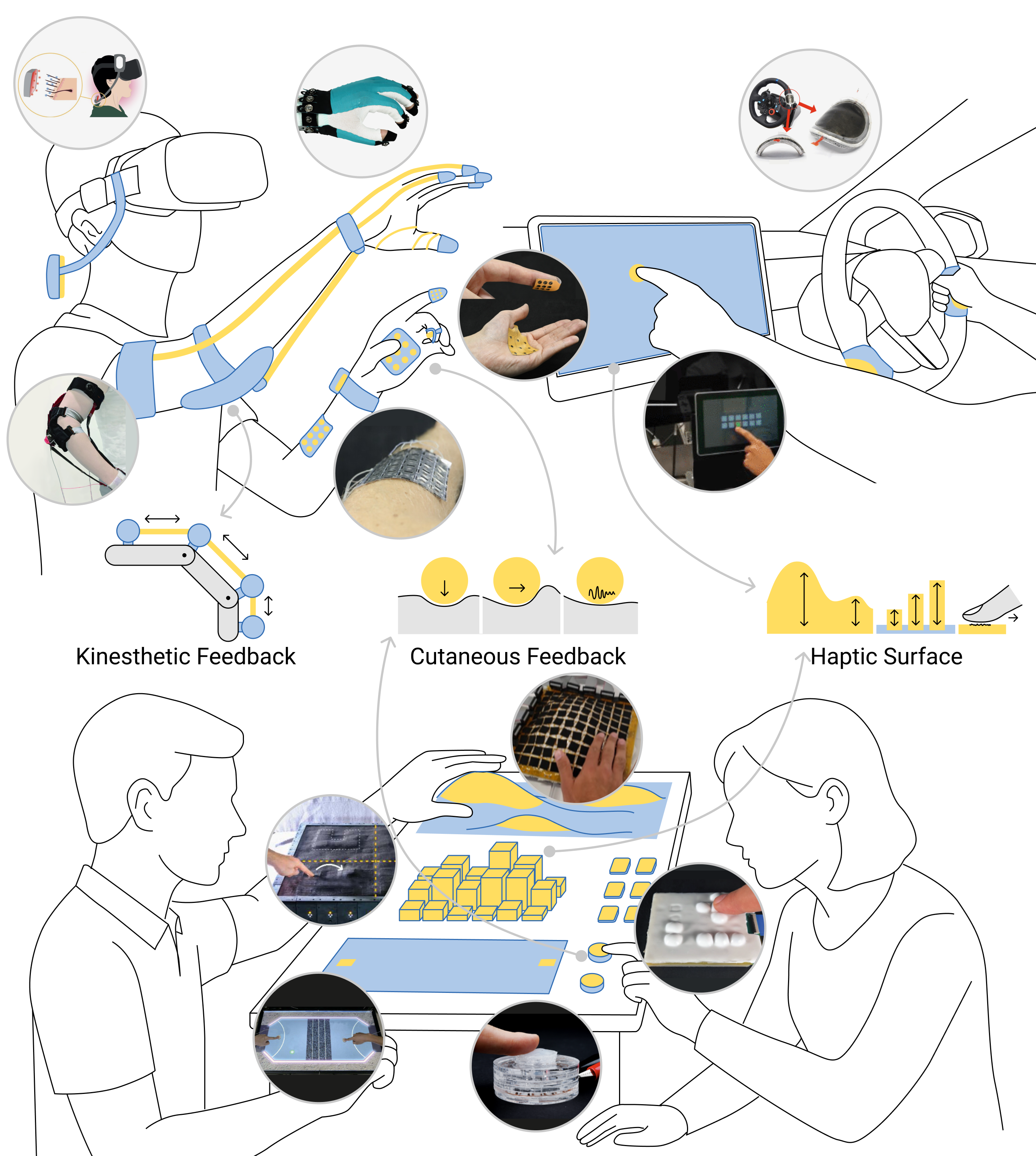
Power from Potential: A Survey of Electrostatic Actuators for Haptics
arxiv.org
July 22, 2026, 1:03 p.m.
High-Voltage Electrostatic Actuators (HVEAs) represent a promising advancement for haptic interfaces integrated into wearables and everyday environments, addressing limitations of conventional actuators like DC motors and shape memory alloys. HVEAs generate force by applying electric fields to localized charge concentrations using high voltages and ultra-low currents, delivering fast, silent, and energy-efficient operation within customizable, compliant form factors. This survey examines four major HVEA classes: electrostatic switchable adhesives, dielectric elastomer actuators, soft electrohydraulic actuators, and electrokinetic pumps. The analysis characterizes each technology's bandwidth, force density, and spatial scalability for rendering both cutaneous and kinesthetic feedback across wearable and world-grounded interfaces. The research identifies common design constraints and emerging strategies for improving ergonomics, fabrication, and self-sensing integration. HVEAs are uniquely positioned to advance haptic interaction through their compact, lightweight design and fast response times, making them ideal for on-skin and seamlessly integrated applications, with key research directions needed for practical system implementation.
Share on

NASA reveals city-sized Moon base plans with Blue Origin support
interestingengineering.com
July 21, 2026, 2:47 p.m.
NASA officials described the project as a critical step toward sustained lunar exploration and future missions to Mars. The agency also confirmed new partnerships with private companies, including Jeff Bezos-owned Blue Origin, as it prepares for a planned crewed Moon landing in 2027.
Share on
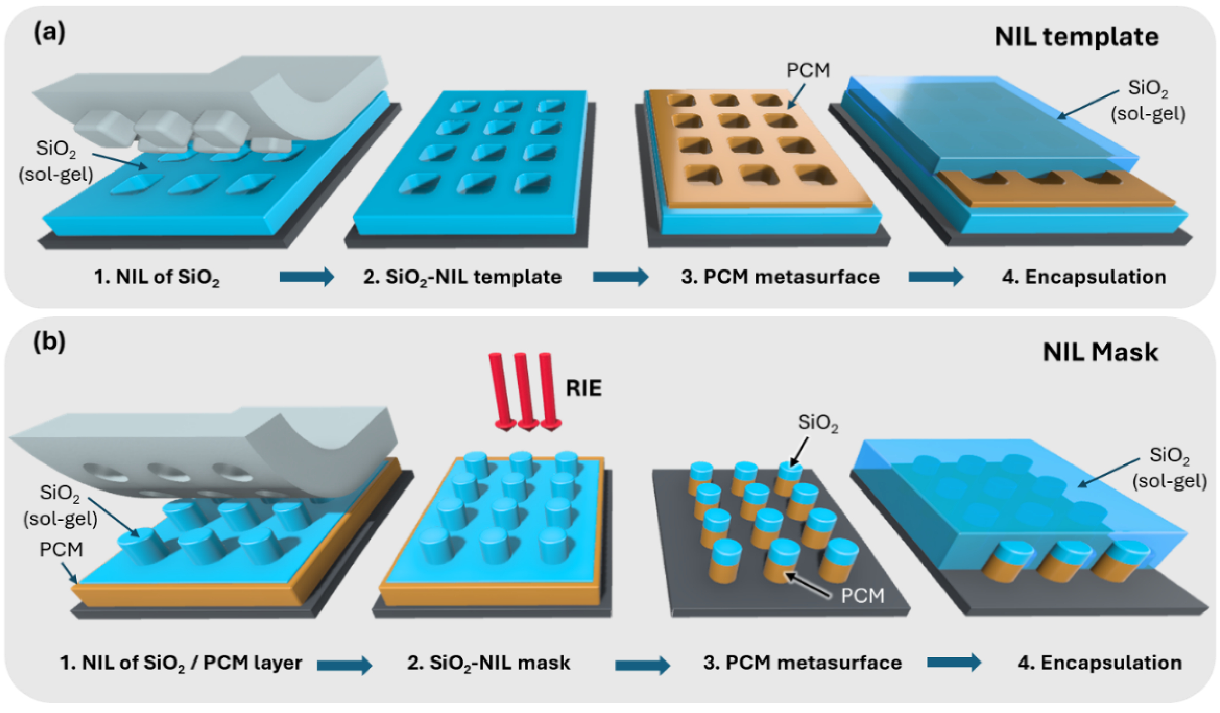
Scalable fabrication of tunable phase-change metasurfaces via soft-nanoimprint lithography
opg.optica.org
July 18, 2026, 4:03 a.m.
Nano-photonic devices based on phase change materials are at the forefront of light management thanks to the electrically or optically tunable response. Their widespread adoption, however, is hampered by the lack of precise, reliable, and scalable fabrication techniques, restricting most demonstrations to proof-of-concept devices. Here we report on scalable approaches for the fabrication of tunable phase-change metasurfaces based on soft-nanoimprint lithography (soft-NIL). Two complementary strategies are showcased: dielectric structures are fabricated by etch-free soft-NIL and used (i) as a template for GeTe deposition or (ii) as etching masks to directly pattern the underlying phase-change material. Both methods enable the realization of centimeter-scale metasurfaces with significantly reduced fabrication complexity compared to conventional lithographic techniques. Reversible switching between melt-quenched and crystalline states is demonstrated using laser-induced phase transitions.
Share on
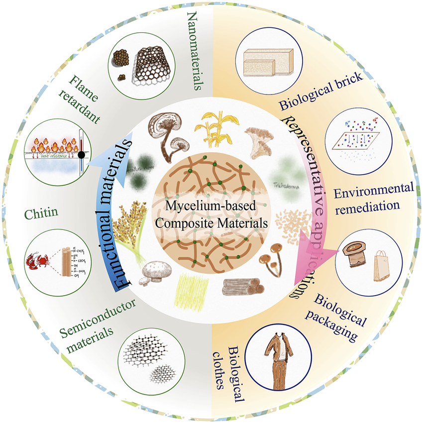
Fungal mycelium-based materials for a new generation of sustainable, bio-based composites
www.igb.fraunhofer.de
July 18, 2026, 4:03 a.m.
Engineered living materials represent an innovative frontier in material science, integrating living cells to create functional components with active properties. Fraunhofer IGB is pioneering fungal mycelium-based systems that leverage growth and self-organization to achieve novel functionalities. These materials offer significant sustainability advantages, being biodegradable and produced from renewable resources. Through additive manufacturing and three-dimensional printing techniques, researchers can achieve precise design and accelerated prototype development. While materials can be deactivated post-shaping to create durable, inert components, the bioactive versions demonstrate promising applications across lightweight construction, biodegradable manufacturing, and advanced bioactive filtration systems, positioning engineered living materials as transformative solutions for sustainable industrial development.
Share on

Microbiome Therapies as an Emerging Therapeutic ...
www.mdpi.com
July 18, 2026, 4:03 a.m.
by V Shapovalov · 2026 — In Australia, access to microbiome therapies is facilitated through regulatory pathways for biological products and special access schemes for experimental ...
Share on

Programmable chemical systems
www.nature.com
July 18, 2026, 4:02 a.m.
To achieve complex and emergent behaviour, chemical systems must be designed to do more than simply express the properties of their individual components. This can be achieved in different ways, from molecular design that encodes specific functions, to reaction cascades, feedback networks, and systems that exploit spatial or temporal organisation. These approaches span many areas of chemistry that are often viewed separately, but are linked by a common goal: to programme chemical behaviour. Examples include oscillating systems that provide temporal control, molecular machines that operate in programmable ways to perform work or deliver a function, and interfaces that introduce compartmentalisation and inhomogeneity into chemical systems.
Share on
Tunable Signal Penetration and Response Plateaus in ...
arxiv.org
July 15, 2026, 1:04 p.m.
Researchers have developed a novel approach to dynamically control mechanical signal processing in soft materials by incorporating internal bistability into metamaterials. The study presents both microscopic simulations and a nonlinear continuum theory demonstrating how bistable elements can actively modulate response and signal attenuation. The research reveals two key phenomena: a universal screening mechanism that reduces signal penetration at high driving frequencies, and a frequency-insensitive response plateau emerging from timescale separation. The model offers closed-form analytical solutions enabling quantitative design rules. Critical findings show that conformational length changes primarily control attenuation strength, while switching rates tune the attenuation regime and plateau position. However, a fundamental design trade-off exists where larger conformational changes enhance dissipation but increase energy barriers, risking state-locking. Optimal signal attenuation emerges from balancing pronounced bistability with surmountable transition barriers, providing valuable insights for advancing soft robotics and mechanosensing applications.
Share on

Biomimetic gradient hydrogels for osteochondral ...
www.frontiersin.org
July 15, 2026, 1:04 p.m.
Osteochondral defects present significant clinical challenges due to the complex architecture of cartilage and bone with limited regenerative capacity. Gradient hydrogels represent a promising biomimetic approach that replicates the structural, mechanical, compositional, and biochemical transitions from cartilage to subchondral bone. This comprehensive review examines recent advances in gradient hydrogel design, covering fundamental principles including porosity, stiffness, mineral, and growth factor gradients. It evaluates fabrication strategies such as layer-by-layer assembly, 3D bioprinting, and microfluidic generation, alongside material selection encompassing natural and synthetic polymers with ceramic composites. The review explores biological mechanisms directing cell fate through mechanotransduction and growth factor delivery, synthesizes preclinical evidence demonstrating superior outcomes for gradient scaffolds, and addresses current limitations in durability and translational potential for osteochondral regeneration.
Share on

FSA publishes new guidance to help cell-cultivated food ...
www.proteinproductiontechnology.com
July 15, 2026, 1:04 p.m.
The Food Standards Authority has released updated guidance to support the development and commercialization of cell-cultivated food products. This regulatory framework aims to clarify requirements for manufacturers entering this emerging sector, addressing safety standards, labeling protocols, and approval processes. The guidance reflects growing industry interest in cultivated meat and protein alternatives as sustainable food solutions. By establishing clear regulatory pathways, the FSA seeks to facilitate innovation while maintaining consumer protection and food safety standards. This initiative supports the broader transition toward alternative protein production methods and demonstrates regulatory commitment to emerging food technologies.
Share on

3D Printed Artificial Muscles Advance Soft Robotics
www.plasticsengineering.org
July 15, 2026, 1:04 p.m.
Three-dimensional printing technology is revolutionizing soft robotics by enabling the development of advanced artificial muscles that overcome traditional manufacturing constraints. Researchers have engineered two innovative material systems to replace conventional rigid actuators: electromechanical PVC gel muscles that respond to electrical fields between 400 and 800 volts, and thermomechanical shape-memory polymers activated by thermal triggers. The PVC gel formulation, combining polyvinyl chloride with plasticizer and solvent in precise ratios, generates Maxwell forces that induce controlled deformation and recovery cycles. These polymers leverage molecular switching and entropic recovery mechanisms to achieve programmable actuation. By eliminating labor-intensive manual casting and hardware assembly, three-dimensional printing facilitates the production of highly flexible, autonomous robotic systems with enhanced performance capabilities and design freedom previously unattainable through conventional manufacturing methods.
Share on

What are Indoor Vertical Farms?
www.pubs.ext.vt.edu
July 15, 2026, 1:03 p.m.
Indoor vertical farms represent an innovative agricultural approach that cultivates crops in vertically stacked layers within controlled indoor environments. This farming method optimizes space utilization by growing plants in climate-controlled facilities using artificial lighting, hydroponic or aeroponic systems, and precision nutrient delivery. Indoor vertical farms eliminate dependence on weather conditions and seasonal constraints, enabling year-round production of fresh vegetables, herbs, and leafy greens. This technology significantly reduces water consumption compared to traditional agriculture while minimizing pesticide use and transportation distances. By bringing food production closer to urban centers, vertical farms enhance food security and sustainability while supporting local food systems and creating economic opportunities in urban areas.
Share on

Voici BeFC, la prometteuse pile française qui carbure au sucre, sans le moindre gramme de métal
www.clubic.com
July 13, 2026, 10:12 a.m.
Sans lithium, ni cobalt, ni plomb, depuis Grenoble, la start-up française BeFC a mis au point une pile électrique entièrement dépourvue de métal. Elle explique à Clubic comment le sucre pourrait bien remplacer certaines batteries classiques.
Share on

The Economist tacle l’IA avec intelligence dans sa dernière campagne
creapills.com
July 13, 2026, 9:12 a.m.
Pendant que l’intelligence artificielle inonde le web de contenus générés à la chaîne, The Economist choisit un terrain radicalement inverse : l’affichage physique, dépouillé, pensé pour l’intelligence humaine. L’hebdomadaire britannique déploie une nouvelle série out-of-home aux États-Unis et au Royaume-Uni, signée par l’agence indépendante australienne Cocogun, basée à Sydney.
L’angle n’a rien d’accessoire. À l’heure où la désinformation et les textes synthétiques circulent plus vite que les faits, le titre se positionne comme un rempart : facts, contexte, insight. Un contrepied assumé, qui transforme la lutte contre le bruit informationnel généré par l’IA en argument de marque.
Share on

En Colombie, plus le logo de cette marque de bière est gros, moins le maillot coûte cher
creapills.com
July 13, 2026, 9:12 a.m.
Le maillot 2026 de la sélection colombienne est le plus cher de l’histoire du pays : 150 dollars, soit près d’un quart du salaire mensuel moyen. Résultat, de nombreux supporters renoncent à porter la célèbre tunique jaune, faute de moyens. Un problème d’accès qui touche directement le lien entre une nation et son équipe.
Share on

Top emerging UK food innovations: 2025-2035
www.gov.uk
July 12, 2026, 12:41 p.m.
This UK Food Standards Agency and Food Standards Scotland publication outlines emerging food innovations anticipated to influence the food system between 2025 and 2035. The document examines innovative food technologies expected to reach UK markets during this period, providing regulatory guidance and authorisation routes aligned with the Government's National Vision for Engineering Biology. Market authorisation decisions remain subject to evidence-based legal processes assessed individually, with arrangements varying between Great Britain and Northern Ireland. The initiative supports the UK's £2 billion bioeconomy investment over ten years, including dedicated funding for regulatory assessment of novel food technologies.
Share on